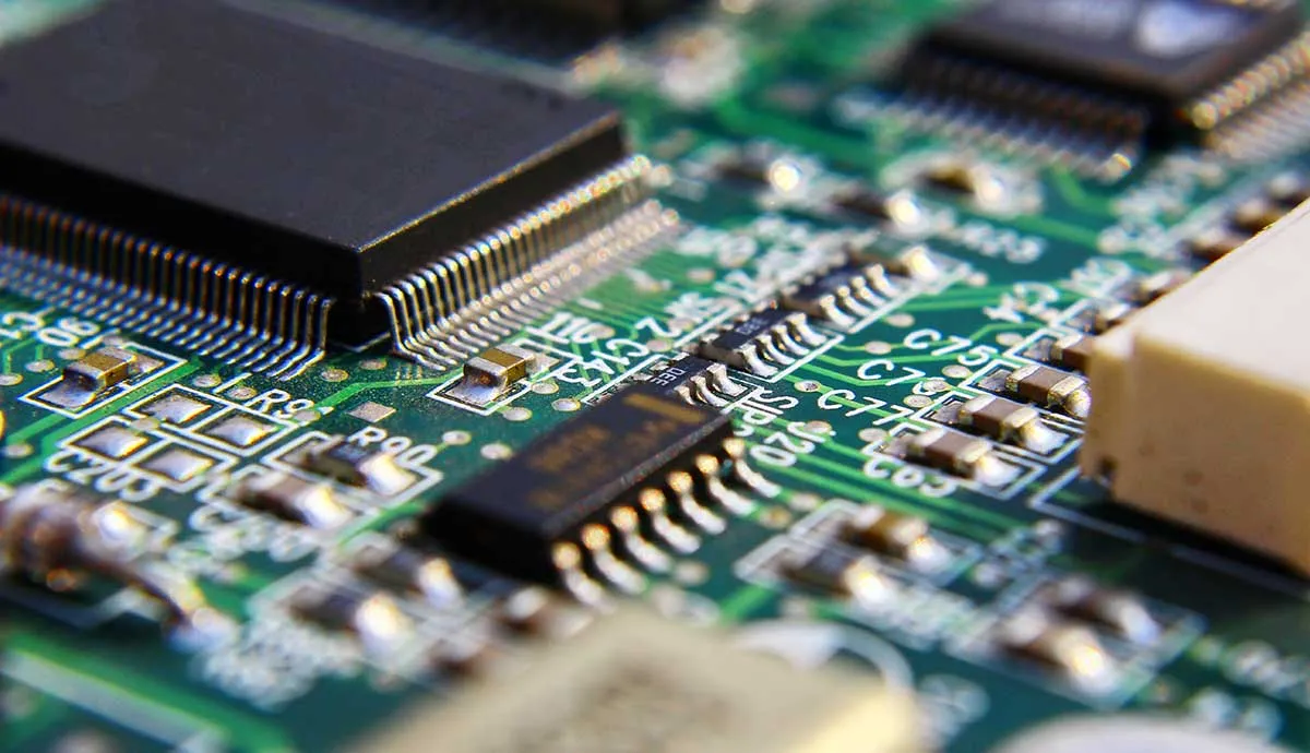
Silicon wafers and semiconductors are essential for creating electronic chips used in many modern technologies, such as phones, watches, cars, medical devices, and more. A wafer, also known as a slice or substrate, is a thin piece of semiconductor on which electronic chips are fabricated. These components and the materials they are made from and packaged with are highly fragile and sensitive to dirt, dust, static electricity, chemical impurities, moisture, temperature, impact, and more. Therefore, creating ultra-pure static dissipative packaging to manufacture and safely transport sensitive electronic components is extremely challenging. This article will discuss the increasing demand for specialized polymer packaging for semiconductors, the challenges faced by the industry, potential solutions to these challenges, and how Avient can help.
Increased Demand for Specialty Polymer Solutions and Materials for Semiconductor Packaging
The demand for data center infrastructure has significantly increased with the accelerated adoption of AI-based solutions, cloud computing, and big data analytics. These technologies rely on semiconductors to process data and provide cloud computing power. This has boosted demand for silicon wafers and semiconductors used in servers, storage devices, and networking equipment. According to a report by Fortune Business Insights¹, the global data center market size was valued at USD 219.23 billion in 2023 and is projected to grow from USD 242.72 billion in 2024 to USD 584.86 billion by 2032, exhibiting a CAGR of 11.6%., resulting in an increased demand for specialty packaging to safely transport silicon wafers and semiconductors.
Challenges:
A speck of dust or dirt is like a mountain on an electronic chip and can significantly degrade performance. Chemical impurities or static discharge can do the same. Therefore, creating ultra-pure, statically dissipative, and safe packaging is crucial for protecting silicon wafers and semiconductors during manufacturing and transport. To meet this demand for quality packaging, ultra-pure static dissipative specialty engineered polymers, and the facilities that manufacture them require specific cleanliness and strict environmental controls. Additionally, finding specialty solutions and materials manufacturers that can provide high-quality raw materials, support global supply chains, and have specific facilities available to manufacture these materials are keys to success.
Solutions:
To achieve this high level of protection, maintaining stringent quality controls and cleanliness standards for manufacturing the semiconductor packaging materials and the packaging is crucial. The polymer solutions and specialty-engineered polymers utilized within the packaging require advanced static dissipative properties to protect electronic components from electrostatic discharge (ESD) and environmental variations. This requires developing manufacturing facilities equipped with ultra-clean feeders, deionized water systems, and specific HVAC systems to ensure the highest levels of cleanliness and control ionic and metal contamination down to parts per billion (PPB). As a result, the materials within the facility, including the air and water quality, matter as much as the personal protective equipment (PPE) materials that a worker in the facility is wearing.
How Avient Can Help
Avient’s ultra-pure Stat-Tech™ Static Dissipative Formulations are polymeric formulations that combine select engineered resins with conductive additives such as carbon powder, carbon fiber, nickel-coated carbon fiber, and stainless steel fiber, that provide the precise level of electrical conductivity required for your application. Depending on your application’s performance needs, Avient can develop a custom Stat-Tech formulation to provide anti-static properties, dissipation, conduction, and electromagnetic and radio frequency interference (EMI/RFI) shielding.
Equally important to providing advanced ESD materials, we possess a deep understanding of the necessary controls to safeguard the purity of the entire manufacturing process. Avient's global specialty manufacturing footprint and ability to source high-purity raw materials can also help meet increased cleanliness requirements. Additionally, Avient has made strategic investments in select facilities in Asia and the US with specialized production lines and stringent cleanliness standards, including the capability to measure purity resolutions down to PPB. These increased efforts allow us to manufacture these critical materials and translate solutions and services globally.
Avient can be a strategic innovation partner in this high-paced, high-innovation application market. Connect with an expert here.
Citations: ¹Fortune Business Insights "Data Center Market Regional Forecast, 2024-2032" https://www.fortunebusinessinsights.com/data-center-market-109851
